The thin blue lines you see when you open up the KiCAD PCB Editor are ratlines. They show which pins still need a copper trace between them based on your schematic. Every time you tweak the schematic, click the Update PCB from Schematic to refresh them.
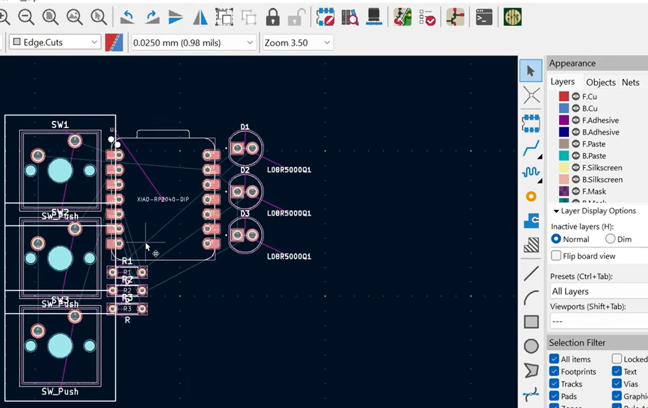
Hover over a pad and click X to route that net. As long as your schematic is right, you can trust the ratlines on where you should route your traces.
When a trace needs to go from the front to the back (or vice versa), you’ll drop a via , a small plated hole connecting the layers. Use them, but don’t go overboard (we shouldn’t be seeing 40 vias on a two-sided board).
Routing tips and conventions
- No 90° trace corners. Use 45s or curves instead , they’re much friendlier to manufacture.
- Keep angles obtuse, not acute wherever a trace curves.
- Limit vias. Every one adds cost and a small amount of signal loss.
- Keep signal traces on one layer where you can.
- Drop ground pours on empty board space instead of leaving it bare copper, cleaner power, less noise.
- Vary trace widths by current. Thin traces are fine for signals; anything carrying real power (3v3, LED arrays) wants a noticeably wider trace.
Tools → Design Rules Checker. This will tell you if you have any obvious errors with your board. Do this all the time! Also, make sure you’re hitting CTRL+S to save your PCB!
Helpful Links
To make sure your design isn’t going awry
- docs.kicad.org, the official KiCAD manual
- altium.com/documentation, some of the best plain-English writing on routing and signal integrity out there
Silkscreen art
Once your routing’s done, have some fun with the silkscreen (the yellow/pink layer used for text and art) on the front and back of your board. Add your name, your board’s name, a picture of your dog, the Runtime logo, anything!
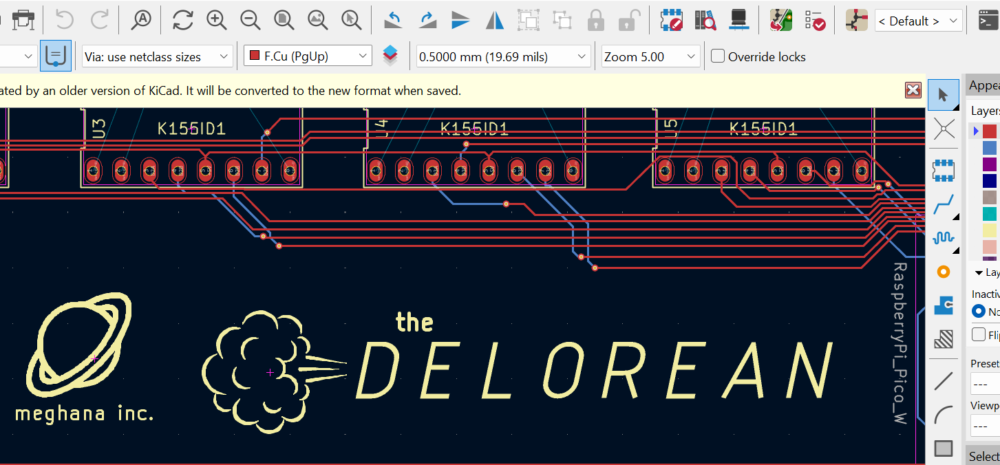
Open the KiCAD Image Converter, drop an image logo in, and it’ll give you a footprint you can place directly. You’ll probably need to mess with the size to make it fit like how you want.
Once you’re done routing, post a screenshot of your PCB in #runtime. This is a quick progress check, you now have a super cool PCB!